Copper has been historically used by humans since tens of thousands of years ago and hence has a historical significance is the domain of metallurgy. Being a metal, whose alloys have been explored and tuned for millennia, copper alloys are known for their thermal and electrical conductivity, and ductility. For example, bronze is an alloy of copper that has been the most explored metal in the aptly named Bronze Age. Additionally, their corrosion resistance, strength, and their abundance make them valuable for many industries.
Metallography
of Copper Alloys
Contents
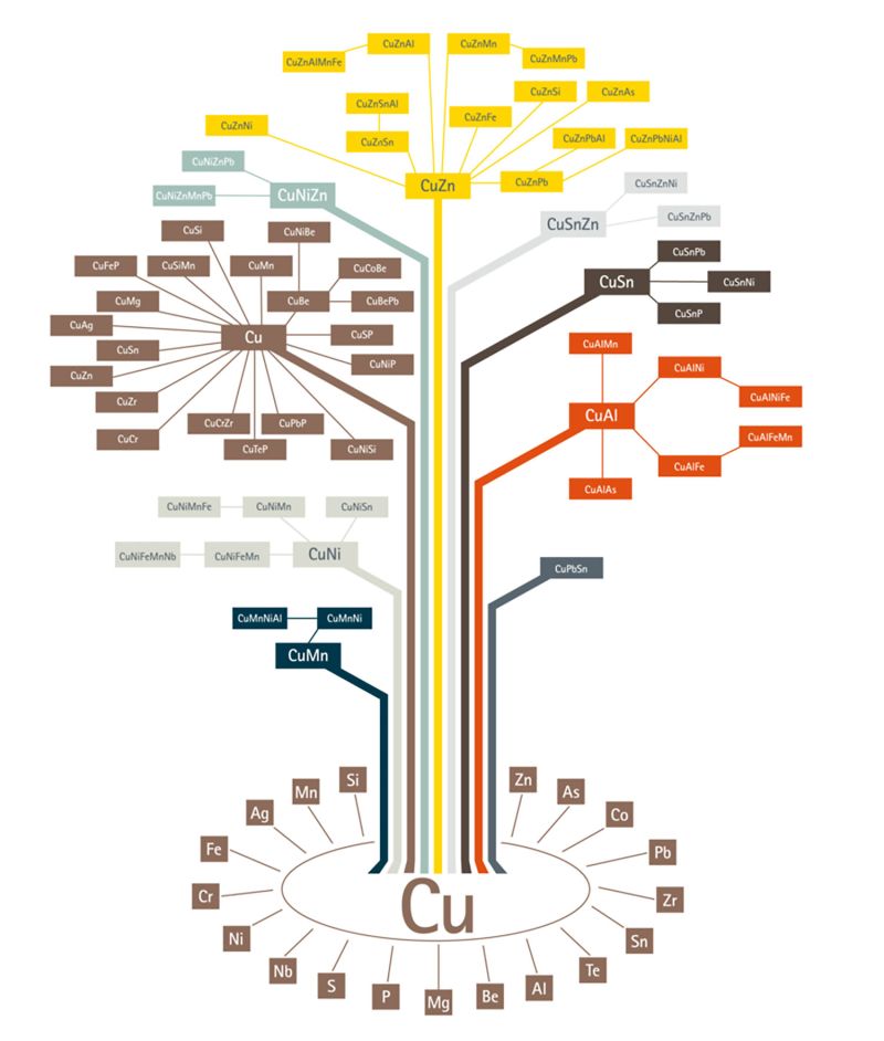
Today, there is a plethora of copper alloys in the market from which, one can choose the right grade depending on the properties required. The copper alloy tree published by the European Copper Institute gives a broad picture of copper alloys in existence. As it could be seen from the alloy tree, copper can be alloyed with a variety of other metals. Broadly, there are 6 categories of copper alloys used extensively:
- Brass – Alloyed with Zinc
- Bronze – Alloyed with Tin
- Copper-nickel – Alloyed with Nickel
- Nickel Silver – Alloyed with Nickel and Zinc
- Gunmetal – Alloyed with Tin, Zinc and Lead
- Copper Beryllium – Alloyed with Beryllium
It should be noted that, unalloyed pure copper also is used for many electrical applications. Regardless of the alloy of interest, metallography plays a critical role in qualifying an alloy for an application and also, in developing new alloys for certain applications.
1/ Metallography
Copper alloys can be wrought or cast. Being ductile, they can be cold- or hot- rolled easily relative to other conventional non-ferrous alloy systems. Depending on the manufacturing technique and the treatment they are subjected to, one can extract several important inferences from microstructural characterization. In brass and bronze alloys for example, deformation from extruding results in extensive formation of ‘twins’ in the microstructure. The picture below shows how twins reveal themselves in a rolled brass alloy. Care has to be taken to not induce any deformation while preparing the sample.
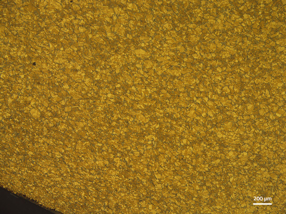
Depending on the treatment parameters the alloy is subjected to, such as annealing temperature, grains can recrystallize or grow. When the temperature distribution in the part is not uniform, the grains sizes can vary. The same phenomenon can occur from extrusion or rolling loads. Considering that copper alloys deform easily, the grain size variation can play a critical role in deciding the mechanical properties of the final part.

Copper alloy microstructures can contain a wide range of phases represented by greek alphabets. The presence of a particular phase depends on the alloy system and the fabrication method. Among the various phases, α-phase can be considered principal as it indicates the FCC (Face centered cubic)-structure of copper at equilibrium. When all the alloying elements are dissolved in the copper matrix, which is usually the case in Cu-Ni systems, one observes a single phase of α. However, adding elements can promote formation of other phases giving rise to polyphase microstructures. For example, raising the composition of tin above 11% in cast tin-bronzes can result in polyphase microstructures with islands of δ-phase (a tin-rich FCC-structured phase). Shown below is a polyphase microstructure of a cast bronze alloy.
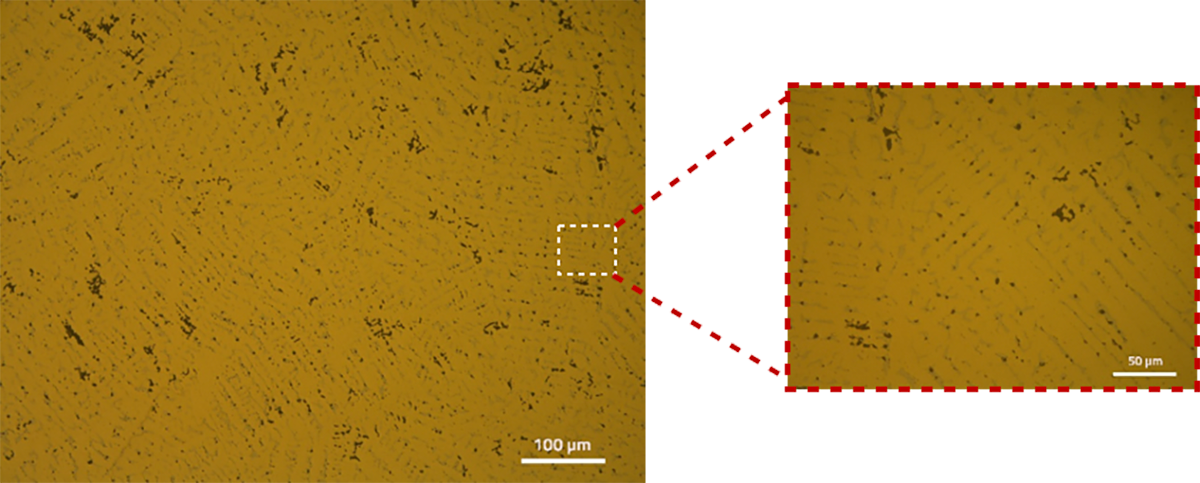
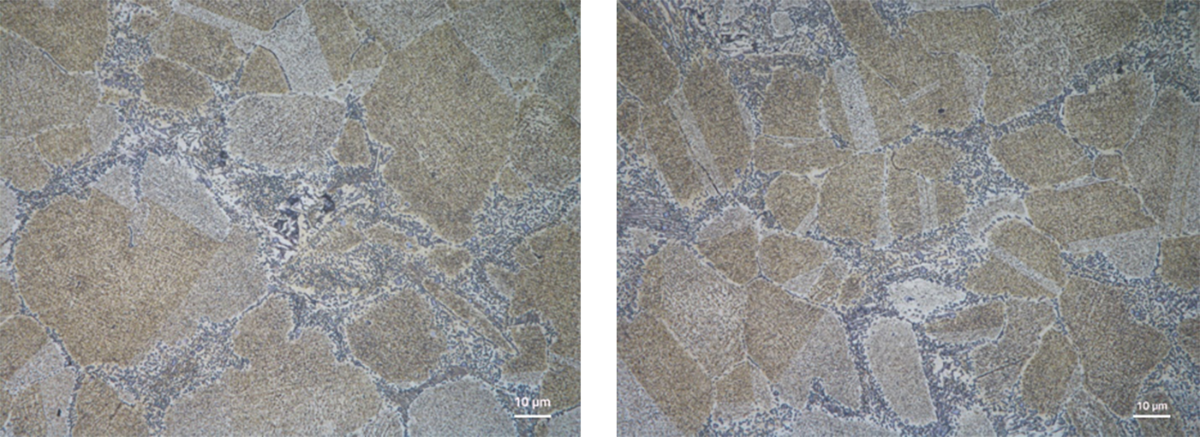
Intermetallic precipitates as seen in the microstructure above, in the intergranular regions, can be disastrous for structural applications. For certain applications, the precipitates are advantageous designed to refine grain sizes. Whichever the case, metallography gives critical cues in the morphology and characteristics of such precipitates.
One principal factor affecting the conductive properties of pure copper is the amount of oxygen it contains. Oxygen can also profoundly change the microstructure of the alloy. It is interesting to note that, copper and oxygen form a eutectic system like the Cu-Al alloy systems.
2/ Sample preparation methods
In order to analyze the microstructure, the sample has to prepared without damaging the microstructure.
Here below are the methods to follow during each step in the sample preparation process to properly analyze the microstructure.
- Cutting
- Mounting
- Polishing
Cutting
While preparing a metallographic sample, the regions of interest have to be chosen carefully. Once the region is chosen, the cutting consumables, machine and holding systems can be rightly chosen. Often multiple cuts are required to separate the region of interest.
Cutting wheels
For rough cutting LAM PLAN Excellence wheels can be used. For precision cutting applications, LAM PLAN Precision cutting wheels are recommended. For more advice on cutting consumables and parameters refer to our posts on the metallography of specific material being cut.
For copper alloys, Excellence H4 and Precision White wheels would be appropriate choices. These wheels contain SiC abrasives in them making them the preferred choice for sectioning copper alloys
Fixing the workpiece
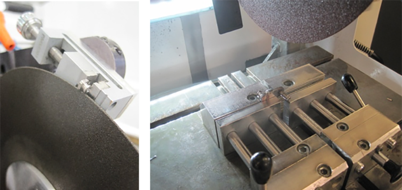
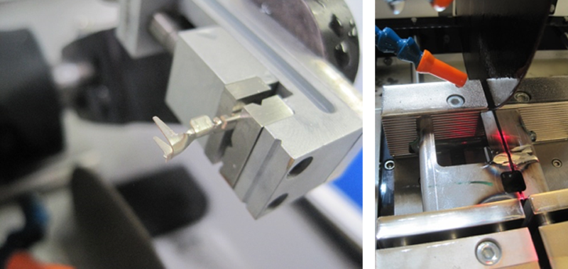
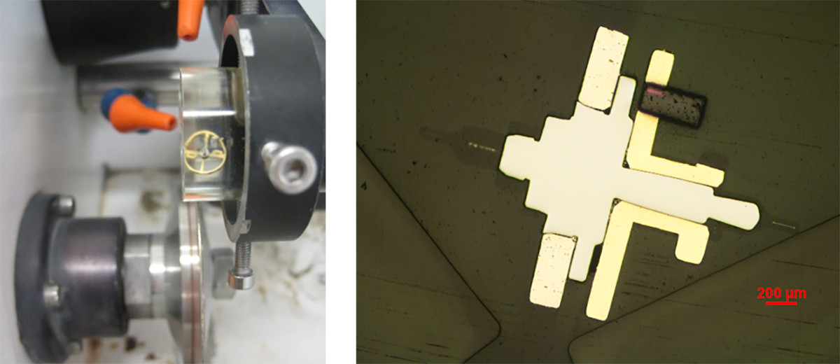
Depending on the form and size of the workpiece, a vise or a fixation system should be chosen. The complex shapes of some parts can add complications to this process. Sometimes, when the part is intricately complex, it is mounted in a resin before cutting. LAM PLAN’s fixation systems avoids excessive vibrations and dangerous release of pieces from the fixation systems while cutting with Cutlam machines.
Cutting fluid
For non-ferrous alloys, LAM PLAN Cutting fluid 723 is recommended to be used to avoid excessive heating and microstructural deformation. The fluid provides the right proportion of lubrication and cooling effect making it ideal for metallographic applications.
Mounting
Copper alloys can be sensitive to temperatures above 150oC which is generally attained in hot mounting processes. Depending on the thermal sensitivity of the information to be interpreted from the microstructure, hot mounting or cold mounting can be chosen.
LAM PLAN’s widely used CMR-free 605 resins can offer quick and easy-to-use cold mounting solutions. When edge retention becomes critical, polyester-based resin 607 or CMR-free epoxy resins 603 and 603.2 works effectively.
When the piece is to analyzed under an SEM, special conductive resins are available. Alternatively, one could use a general-purpose mounting resin and gold-sputter the surface after polishing.
To know more about all our mounting consumables:
Grinding and Polishing
The first step is usually coarse grinding to render the samples flat. SiC papers are widely used for grinding copper alloys as they offer fast material removal.
Once the samples are flat, they can be pre-polished/polished. LAM PLAN TouchLam 2TS3 and 3FV1 are very effective when used with Neodia abrasives on copper alloys. The pads also maintain the samples flat during the polishing process.
Often, this polishing step is supplemented by a finer polishing step to refine the scratches further to analyses the microstructure are higher magnifications (>200X) or even an SEM (Scanning Electron Microscope). This step can be definitely skipped when only relatively large features are being analyzed.
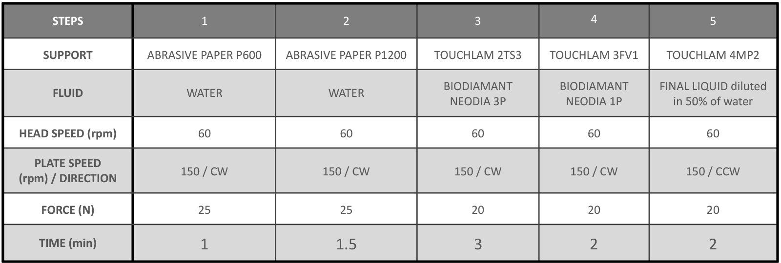
CW – Clockwise / CCW – Counter Clockwise / Head direction: CW (the procedure is presented of polishing 6 mounted samples of diameter 30 mm)
For advice on polishing steps, refer to our posts on metallography of specific materials:
3/ Troubleshooting
Listed below are some solutions to common problems that can arise during metallographic sample preparation of copper alloys.
-
Burn marks on cut surface
-
Cause(s)
• Feed speed too high
• Wrong choice of cutting wheel
• Insufficient coolant flow -
Solution(s)
• Check if the cutting wheel is right for the material being cut
• Reduce the feed speed
• Focus the coolant on the cutting region. If necessary replace the coolant.
-
Excessive relief around porosities and defects
-
Cause(s)
• Long polishing times on a napped cloth
-
Solution(s)
• Reduce polishing time with colloidal silica
-
Scratches persist on microstructure after final polishing
-
Cause(s)
• Contamination of polishing pad
• Improperly cleaned samples after pre-polishing
• Gap between mount and the sample -
Solution(s)
• Replace the polishing pad. Store the polishing pad in a closed cupboard/BoxLam
• Rinse the samples well after each polishing step. Use Ultrasonic cleaner before final polishing
• Try Epoxy resins to avoid gap around the specimen
-
Embedded abrasives after polishing
-
Cause(s)
• Excessive usage of abrasive slurries
• Excessive force while polishing -
Solution(s)
• Reduce abrasive dosing frequency
• Reduce polishing force
-
Smeared layer on the surface
-
Cause(s)
• Improper drying after polishing
-
Solution(s)
• Use alcohol to clean the surface
• Blow dry the surface thoroughly after cleaning
• Use LAM15 for wiping the surface
-
Non-uniform etching of the sample
-
Cause(s)
• Wrong etchant/etching technique
-
Solution(s)
• Choose the right etchant and technique for your alloy (Ref.: ASM Handbook)

